


In the future, there will be a point to where the number of active and passive components that can be physically mounted onto a PCB will exceed the available real-estate of assembly. When this occurs the PCB must increase in size or have features removed, unless we go to stacked assemblies with some form of interconnect between boards. To think about where the future of PCB technology could end up, we can expect the following to become a routine process during development and production. Most PCBs with any level of high technology will be multi-layer using very thing laminates, expensive core material plus various grades of copper depending on roughness and frequency range of operation.
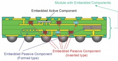
- Discrete active components will be embedded internal to the assembly. Embedding active devices minimizes loop inductance and allows for more real estate on both top and bottom for components and interconnects that cannot be embedded.
- Discrete passives, such as resistors (Ohmega layer), capacitors and inductors will also be embedded along with buried capacitive layers to ensure a high quality power distribution network.
- Transmission lines may end up being fiber optic and not traditional copper. Fiber optic transmission lines are made by placing glass beads in a trench routed out within a core layer during manufacturing and then melted into a fiber optic interconnect.
- Three dimensional components will be used with higher number of I/O pins and greater power consumption known as System on Package (SoP).
Please follow and like us:
Leave a Reply