Engineering Analysis (Frequency or Time Domain)
During consulting assignments, I observe that engineers sometimes struggle to achieve compliance. This not only includes regulatory but functionality. The more senior one is at design engineering, there is the tendency to do things in a manner that is familiar to them. What has been known to work no longer applies with advances in technology, especially the speed of components along with higher levels of complexity in smaller packages or stacked assemblies. Time, money and extended effort are now spent to solve what is probably a simple design or layout problem that is so obvious that one cannot find it quickly.
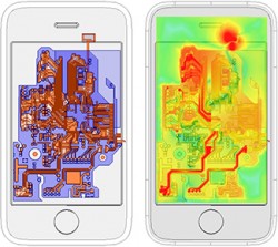
If one had knowledge on advances in semiconductor manufacturing and its effect with regard to high-speed signal integrity along with creation of unwanted common-mode current due to losses in transmission line routing, our job becomes easier. Most EMC engineers are comfortable using a spectrum analyzer to isolate problem areas on a printed circuit board and then go into trial and error mode of fixing the problem by randomly picking out ferrite beads or a decoupling capacitor style or value without understanding what is required, or if these parts are even appropriate.
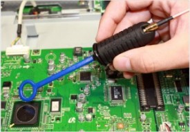
Whenever I get called to troubleshoot an EMI problem at the printed circuit board level, I prefer to use an oscilloscope to locate the actual source location and dig into the physics on what happened that created unwanted EMI. If one understands the fundamentals of “EMC Made Simple“, finding a simple solution is easy. A spectrum analyzer only tells us there is an RF field present, not what created the undesired common-mode RF energy.
In order to understand circuit analysis and transmission line theory as it applies to printed circuit board design and layout in the time domain, continued education is required. There are many places to learn this knowledge that includes seminars (even at your own expense since many employers refuse to pay for training as it affects their revenue bottom line), attendance at conferences, reading technical papers and networking with others experts in your local IEEE Chapter or other professional venues. The manner in how you obtain continued education is up to you, as long as you stay current with technology and advanced from research on physical aspects of printed circuit board layout due to higher speed signaling. If you are not willing to pay for training out of your own pocket, then do you deserve to be employed at a company that is willing to replace you with someone else with more knowledge, usually at lower cost?