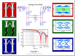
Engineers are facing new challenges related to the design of printed circuit boards (PCBs) and their integration into an enclosure, either metal or plastic. These challenges will increase in the future with higher speed components. With the need to maximize functionality while at the same time shrinking the physical size and weight along with lower cost, we are discovering that signal integrity is becoming a greater concern than EMC. If a PCB does not work as required due to a design flaw in the schematic or component operation, does EMC compliance matter? The product cannot be made available for sale, signal integrity wise.
Although a printed circuit board is the source of undesired radiated or conducted EMI somewhere within a broadband environment of use, will this EMI be a concern in the future, or should we enhance immunity protection against any and all electromagnetic threats that may occur such as electrostatic discharge (ESD), surge and transient events or the presence of large electric and magnetic fields from nearby system?
System and PCB designers, along with EMC engineers, must understand multiple aspects of doing a PCB layout in a manner that ensures not only functionality in the time domain (signal integrity) but also EMC compliance in the frequency domain as they are “exactly” the same thing, just viewed differently. The magnitude of a signal integrity problem due to losses within any transmission line becomes the magnitude of common-mode RF current that is developed, and this undesired current will propagate somehow by either radiated or conducted means.
It is easier to work in the time domain instead of the frequency domain when isolating the source of common-mode energy creation during signal propagation. A transmission line, commonly called a trace on a PCB, allows signal to travel from a source to load through a medium such as free space or metallic interconnect. During signal propagation, we must ensure the following for enhanced signal integrity performance and compliance.
- There must be no loss in any parametric value associated with signal propagation (voltage, current, propagation delay, timing, edge rate distortion, jitter, impedance discontinuities, crosstalk, etc.).
- If the transmission line is perfectly lossless in the source path, RF return current will be equal and opposite within the return path, called differential signaling, providing there is close coupling between the two transmission lines.
- If there is significant loss in either the source or return propagation path, undesired common-mode EMI is developed. This energy will propagate by any antenna structure available in the board, either a magnetic field loop or electric field dipole antenna.
In the future, engineers must learn about the following sample list of signal integrity concerns: Incorrect transmission line routing; improper terminations; power and/or return plane bounce; rise time degradation; lossy lines at high frequencies due to board material selection; hidden parasitics (RLC); skin depth losses; dielectric loss in the board material; propagation delays due to high dielectric constant board material; crosstalk; excessive inductance in the transmission line routing; Delta-I noise; overshoot and undershoot; IR drops; copper roughness; anisotropic aspects of the board material; RoHS (affects delamination and creates tin whisker), to name a few parametic values.
We now come back to the theme of this post….”Should we be more concerned about signal integrity or EMC compliance” during the design cycle?


Leave a Reply